
Request More Information

Email:  WhatsApp:

koenig-logo

Master PCB Design (Electronics) Certification

Master schematic capture, PCB layout, and documentation using Altium Designer. Koenig Solutions provides hands-on labs and real-world projects for the PCB Design (Electronics) course certification.

Browse Courses
certified professional certified professional certified professional certified professional certified professional

500K+ certified professionals

Trusted by enterprise teams at 500+ global companies
From Fortune 500 enterprises to fast-growing tech firms — Koenig alumni are everywhere
Google
Microsoft
Adobe
Dell
HP
Infosys
TCS
Wipro
HCL Technologies
Cognizant
EY
PwC
McKinsey & Company
Bain & Company
HSBC
Shell
Chevron
Saudi Aramco
Bharat Petroleum
GE
Fujifilm
DHL
Emirates
NTT
NHS
United Nations
Capgemini
Google
Microsoft
Adobe
Dell
HP
Infosys
TCS
Wipro
HCL Technologies
Cognizant
EY
PwC
McKinsey & Company
Bain & Company
HSBC
Shell
Chevron
Saudi Aramco
Bharat Petroleum
GE
Fujifilm
DHL
Emirates
NTT
NHS
United Nations
Capgemini

PCB Design (Electronics)

Explore PCB Design (Electronics) certification and training courses — delivered live by certified instructors.

Vendors
Relevant Technology
Level
Duration
All Courses
Browse all certification courses across Microsoft, Cisco, AWS, CompTIA, VMware and more
Showing 1 courses
Popular
Associate
KiCad PCB Engineering from Circuit Concept to Production
4 days · 32hrs
3,127+ 4.7 USD 1,400
View Course
Let’s Talk

Request for more information

PCB Design (Electronics) Certification Training with Koenig Solutions

Course Overview

What is PCB Design (Electronics)?

PCB Design (Electronics) is the engineering discipline of creating printed circuit boards that electrically interconnect and mechanically support electronic components, enabling reliable and compact electronic systems. It involves translating circuit schematics into physical layouts using specialized design tools, ensuring functionality, manufacturability, and compliance with industry standards. Key components in PCB Design include the Substrate (e.g., FR4) for structural insulation, Copper Layers forming conductive traces and planes, Solder Mask to prevent short circuits, and Silkscreen for component labeling. Advanced implementations involve Multilayer, RIGID.flex, HDI Microvia, and Embedded technologies, with design processes covering stack-up planning, component placement, signal routing, and verification for signal integrity, power integrity, and thermal performance. This technology is for electronics engineers, hardware designers, and PCB layout specialists who develop embedded systems, consumer electronics, industrial controls, and communication devices, enabling them to produce efficient, high-performance circuit boards that meet rigorous production and reliability requirements.

Circuit Fundamentals

Analyze resistors, capacitors, inductors and op-amps in analog and digital circuits

Schematic Capture

Create and validate electronic schematics using EDA tools like OrCAD or Altium

Component Footprints

Match schematic symbols to PCB land patterns per IPC-7351 standards

EDA Tools

Navigate PCB design software for layout, routing and design rule checking

Signal Integrity

Apply techniques to minimize crosstalk, impedance mismatches and EMI in layouts

DFM Principles

Implement design for manufacturability rules based on IPC-2221 and IPC-A-610

Who Should Take This Course?

PCB Design Engineer

Create schematics and layouts for mixed-signal and high-speed digital boards using Altium or Cadence tools

Hardware Design Engineer

Define stackups and routing strategies to ensure signal and power integrity in complex PCBs

Electronics Design Engineer

Implement controlled-impedance routing and differential pair layouts for interfaces like PCIe and DDR

PCB Layout Engineer

Optimize component placement and trace routing for manufacturability and thermal performance

Signal Integrity Engineer

Analyze and resolve crosstalk, impedance mismatches and EMI issues in high-frequency designs

Component Engineer

Develop and validate PCB footprints and padstacks aligned with IPC standards and DFM rules

Career Outcomes

What PCB Design (Electronics) Certification Opens Up For You

Based on industry data from certified PCB Design (Electronics) professionals worldwide

83%

of certified PCB Design (Electronics) professionals secured a salary increase last year

Salary Impact
+24%

Average salary increase reported after obtaining a PCB Design (Electronics) certification

Typical Salary Range (Global)
Entry
$75,000–$95,000
Mid
$95,000–$120,000
Senior
$120,000–$145,000

*Source: Glassdoor / LinkedIn 2025

Job Roles
  • PCB Design Engineer
  • PCB Layout Engineer
  • Hardware Design Engineer
  • Senior PCB Designer
  • PCB Design Manager
  • RF PCB Designer
  • High-Speed PCB Engineer
  • Embedded Systems Designer
  • Signal Integrity Engineer
  • Electronics Design Engineer
Companies Hiring
L&T Technology Services Tessolve Caliber Interconnect Solutions Sienna ECAD Technologies Zettaone Technologies Molex Data Patterns TCS Pactron /HJPC Varroc Group Ammunic Systems Ultrahuman ZF Group Rantronics Technology TechiesDesigns Electronics

and 5,000+ organisations worldwide seeking PCB Design (Electronics) certified professionals

The building blocks every PCB Design (Electronics) solution is made of

01
Allegro X Design Platform
A full-stack engineering environment for multi-board electronic system design. Practitioners build complex PCBs with integrated schematic capture, layout, and analysis workflows.
02
Altium Designer
An integrated PCB design software combining schematics, layout, and simulation. Engineers build complete electronic designs from concept to manufacturing documentation.
03
Xpedition Standard
A scalable PCB design solution for simple to complex board development. Designers build high-performance circuits using AI-powered automation and integrated MCAD workflows.
04
PSpice
A SPICE simulation environment for analog and mixed-signal circuit verification. Engineers build and test circuit behavior before physical prototyping.
05
Manufacturer Part Search
A component search panel with verified manufacturer data. Designers build reliable PCBs using ready-to-place parts with real-time supplier information.
Altium 365 Workspace
This cloud-hosted platform secures your PCB Design (Electronics) projects, components, and BOMs. It provides robust lifecycle management, version control, and real-time collaboration to ensure full traceability across all design stages.
GraphQL API & Connectors
Gain programmatic access to PCB Design (Electronics) data using our GraphQL API. Integrate seamlessly with PLM systems including PTC Windchill, Arena, Agile, Aras, and Teamcenter for efficient bi-directional design synchronization.
Learning Formats

Learning That Fits Your Life

Four formats. One quality standard. Every option comes with the same expert instructors, official courseware, and money-back guarantee.

Classroom Training Most Popular

Classroom Training

Traditional, instructor-led learning in popular global destinations.

Classroom Training

  • Hands-on lab sessions
  • Face-to-face with expert instructors
  • Global training centers
Live Online Classes Best Value

Live Online Classes

Flexible virtual learning with expert instructors from the comfort of your own space.

Live Online Classes

  • Live instructor-led sessions
  • Interactive Q&A & labs
  • Train from anywhere
Fly-Me-A-Trainer (FMAT) Fastest

Fly-Me-A-Trainer (FMAT)

Flexible on-site learning for larger groups. Fly an expert to your location anywhere in the world.

Fly-Me-A-Trainer (FMAT)

  • Expert trainer at your site
  • Custom schedule & pace
  • Any location worldwide
Flexi (Self-Paced) Most Flexible

Flexi (Self-Paced)

Self-paced learning with edited lectures, courseware, hands-on labs, and optional doubt clearing sessions.

Flexi (Self-Paced)

  • Edited video lectures
  • Hands-on labs & courseware
  • Optional doubt clearing sessions
1-on-1 Training Most Focused

1-on-1 Training

Dedicated instructor assigned exclusively to you for maximum personalisation and knowledge retention.

1-on-1 Training

  • Personalised schedule
  • Instructor adapts to your pace
  • Max knowledge retention
Customised Programmes Bespoke

Customised Programmes

Bespoke curricula tailored to your tech stack, business processes, and learning goals.

Customised Programmes

  • Custom course content
  • Fits your tech stack
  • Aligned to business goals
Webinar as a Service New

Webinar as a Service

Professionally hosted live webinars delivered to your global workforce at scale.

Webinar as a Service

  • Global workforce delivery
  • Live hosted sessions
  • Scalable & trackable
Qubits Assessment

Qubits

AI-powered assessments to benchmark skills, identify gaps, and measure training ROI.

Qubits

  • Skill benchmarking
  • Gap identification
  • Training ROI measurement
The Honest Comparison
How Koenig Stacks Up Against Every Alternative

Every factor that determines whether you actually pass your PCB Design (Electronics) exam — rated across every training format available.

Koenig
Official ALP Partner
12
/12 criteria ✓
ALP Provider
Other authorised partner
5
/12 criteria
Legacy Provider
Traditional classroom
2
/12 criteria
Self-Paced Platform
On-demand video
2
/12 criteria
Free Platform
Self-study / free tier
4
/12 criteria
Criteria Koenig ALP Provider Legacy Provider Self-Paced Platform Free Platform Note
Instructor expertise and delivery
Siemens Certified Instructor
Live instructor-led sessions
1-on-1 private training Partial
Siemens EDA Authorization
Official Siemens ALP Status
Official courseware product Partial
ESI / EA Credits Accepted
Flexibility and access
Any-day / flexi start Partial
On-site or fly-me-a-trainer
Global delivery reach Partial
Results and trust
Exam pass rate Row omitted: unverified data for PCB Design (Electronics)
Entry price for fundamentals N/A ~$2,500/year ~$899 $15-30/mo Free
Verified learner reviews Row omitted: unverified data for PCB Design (Electronics)

Data sourced from public pricing pages and review platforms. Accurate as of March 2026. Partial = available in select regions only.

Recognition

Awards & Recognition

Recognized by global vendors and quality bodies for training excellence

10+
Awards & Certifications
6+
Global Partners
15 Yrs
Great Place to Work
Microsoft Partner of Year
Winner of Microsoft Training Services Partner of the Year Award

Winner of Microsoft Training Services Partner of the Year Award

2025
Winner of Microsoft's ANZ Superstar Campaign

Winner of Microsoft's ANZ Superstar Campaign

2024
Winner of Microsoft's Asia Superstar Campaign

Winner of Microsoft's Asia Superstar Campaign

2022
Finalist – AWS Partner of the Year

Finalist – AWS Partner of the Year

2024
Winner of EC-Council ATC of the Year Award

Winner of EC-Council ATC of the Year Award

2024
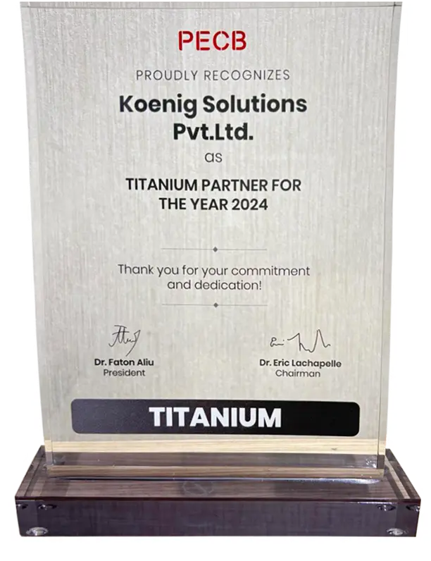
Winner of the PECB Titanium Partner Award

Winner of the PECB Titanium Partner Award

2024
Certified as a Great Place to Work
Great Place to Work

Certified as a Great Place to Work

2011–2025
Winner of RedHat Gold Partner of the Year – Non-Retail (GLS India)

Winner of RedHat Gold Partner of the Year – Non-Retail (GLS India)

2025
Winner of RedHat Gold Partner of the Year – Non-Retail (GLS India)

Winner of RedHat Gold Partner of the Year – Non-Retail (GLS India)

2024
Winner of the Red Hat Partner of the Year Award

Winner of the Red Hat Partner of the Year Award

2023
Reviews

What our 500K+ alumni say

Verified reviews from learners certified on Azure, AI, Security, and more.

18,400+
Verified Reviews
4.9 / 5
Average Rating
95%
Would Recommend
1M+
Professionals Trained
  • ★★★★★

    “Passed AZ-104 on first attempt. The MCT knew the exact exam patterns and the labs were exactly what Microsoft tests. Worth every penny.”

    Rahul M.

    Rahul M.

    Azure Administrator

    AZ-104 Certified

    ✓ Verified
  • ★★★★★

    “I trained 15 of my team members for SC-200. Koenig’s on-site delivery was seamless and all 15 passed within 3 months.”

    Sarah K.

    Sarah K.

    CISO, Financial Services

    Enterprise Client

    ✓ Verified
  • ★★★★★

    “The 1-on-1 format was a game changer. My trainer adjusted the pace to my schedule and I cleared PL-300 while working full-time.”

    Ahmed R.

    Ahmed R.

    Business Intelligence Lead

    PL-300 Certified

    ✓ Verified
  • ★★★★★

    “Passed AZ-104 on first attempt. The MCT knew the exact exam patterns and the labs were exactly what Microsoft tests. Worth every penny.”

    Rahul M.

    Rahul M.

    Azure Administrator

    AZ-104 Certified

    ✓ Verified
  • ★★★★★

    “I trained 15 of my team members for SC-200. Koenig’s on-site delivery was seamless and all 15 passed within 3 months.”

    Sarah K.

    Sarah K.

    CISO, Financial Services

    Enterprise Client

    ✓ Verified
  • ★★★★★

    “The 1-on-1 format was a game changer. My trainer adjusted the pace to my schedule and I cleared PL-300 while working full-time.”

    Ahmed R.

    Ahmed R.

    Business Intelligence Lead

    PL-300 Certified

    ✓ Verified
  • ★★★★★

    “From AZ-900 to AZ-305 in 6 months. Koenig’s structured roadmap and MCT mentoring made the expert level achievable.”

    Priya S.

    Priya S.

    Cloud Solutions Architect

    AZ-305 Expert

    ✓ Verified
  • ★★★★★

    “As an L&D head I’ve used 5 training vendors. Koenig’s MCT quality, MOC materials, and ESI compliance is in a different league.”

    James T.

    James T.

    Head of L&D, UK Enterprise

    100+ Learners Trained

    ✓ Verified
  • ★★★★★

    “SC-900 and SC-300 back to back — both cleared first try. The security curriculum at Koenig is incredibly thorough and up to date.”

    Aisha N.

    Aisha N.

    Security Analyst

    SC-300 Certified

    ✓ Verified
  • ★★★★★

    “From AZ-900 to AZ-305 in 6 months. Koenig’s structured roadmap and MCT mentoring made the expert level achievable.”

    Priya S.

    Priya S.

    Cloud Solutions Architect

    AZ-305 Expert

    ✓ Verified
  • ★★★★★

    “As an L&D head I’ve used 5 training vendors. Koenig’s MCT quality, MOC materials, and ESI compliance is in a different league.”

    James T.

    James T.

    Head of L&D, UK Enterprise

    100+ Learners Trained

    ✓ Verified
  • ★★★★★

    “SC-900 and SC-300 back to back — both cleared first try. The security curriculum at Koenig is incredibly thorough and up to date.”

    Aisha N.

    Aisha N.

    Security Analyst

    SC-300 Certified

    ✓ Verified
  • ★★★★★

    “AI-102 was daunting but the trainer broke it down perfectly. Real Azure OpenAI labs made the difference. Highly recommend.”

    David L.

    David L.

    AI Engineer

    AI-102 Certified

    ✓ Verified
  • ★★★★★

    “DP-600 Fabric certification done in 3 weeks of part-time study. The customised schedule around my timezone was a lifesaver.”

    Mei W.

    Mei W.

    Data Platform Engineer

    DP-600 Certified

    ✓ Verified
  • ★★★★★

    “Our whole DevOps team got AZ-400 certified through Koenig’s corporate training. Smooth logistics and top-tier MCTs throughout.”

    Carlos R.

    Carlos R.

    Engineering Manager

    AZ-400 Team Training

    ✓ Verified
  • ★★★★★

    “AI-102 was daunting but the trainer broke it down perfectly. Real Azure OpenAI labs made the difference. Highly recommend.”

    David L.

    David L.

    AI Engineer

    AI-102 Certified

    ✓ Verified
  • ★★★★★

    “DP-600 Fabric certification done in 3 weeks of part-time study. The customised schedule around my timezone was a lifesaver.”

    Mei W.

    Mei W.

    Data Platform Engineer

    DP-600 Certified

    ✓ Verified
  • ★★★★★

    “Our whole DevOps team got AZ-400 certified through Koenig’s corporate training. Smooth logistics and top-tier MCTs throughout.”

    Carlos R.

    Carlos R.

    Engineering Manager

    AZ-400 Team Training

    ✓ Verified

Got Questions? We've Got Answers.

Everything you need to know about PCB Design (Electronics) certification training with Koenig Solutions.

PCB Design is the process of creating printed circuit boards that provide electrical interconnections and mechanical support for electronic components like ICs, resistors, capacitors, and connectors using copper traces on insulating substrates such as FR4. It involves schematic capture, component placement, routing, and defining the layer stackup with dielectric materials. The design ensures manufacturability, signal integrity, and thermal management for devices ranging from consumer electronics to aerospace systems.
PCB Design training is for electronics engineers, circuit designers, and layout technicians with at least 1–2 years of experience in electronics development. It serves roles such as PCB layout engineers, hardware design engineers, and R&D professionals working on embedded systems, IoT devices, or high-speed digital circuits. The training benefits those transitioning from schematic design to physical layout and those aiming to master HDI, signal integrity, or IPC standards.

Learners need foundational knowledge of electronic circuits, Ohm’s Law, and component behavior, along with familiarity with EDA tools like Altium Designer or Cadence Allegro. Experience in reading schematics and understanding basic manufacturing processes such as soldering and PCB fabrication is essential. Prior exposure to signal integrity concepts or high-speed design is beneficial but not mandatory for introductory courses.
PCB Design training prepares for the IPC CID (Certified Interconnect Designer) and CID+ (Advanced) certifications, which validate expertise in PCB layout, stackup design, materials selection, DFM, and compliance with IPC-2221 and IPC-6012 standards. The CID exam covers design considerations, component technologies, and documentation, while CID+ includes advanced topics like signal integrity, HDI, and RF/microwave design for high-reliability applications.
The IPC CID exam consists of approximately 100 multiple-choice questions with a passing score of 73% or higher, and it must be completed within an 8-hour testing window. The exam evaluates knowledge across 10 domains including materials, fabrication, assembly, thermal management, and documentation. Certification is valid for two years, after which recertification is required through re-examination or continuing education credits.
PCB Design training typically spans 40 hours over 5 days and is delivered via live online instructor-led sessions, 1-on-1 coaching, private batches, or classroom instruction with guaranteed-to-run dates. Koenig offers flexible start options, including self-paced Flexi mode with recorded HD sessions and trainer support. The training includes hands-on labs using industry-standard EDA tools and real-world design scenarios.
Still have questions?
Talk to a PCB Design (Electronics) certification advisor — free, no obligation.
WhatsApp Us

Training Professionals
Across 50+ Countries

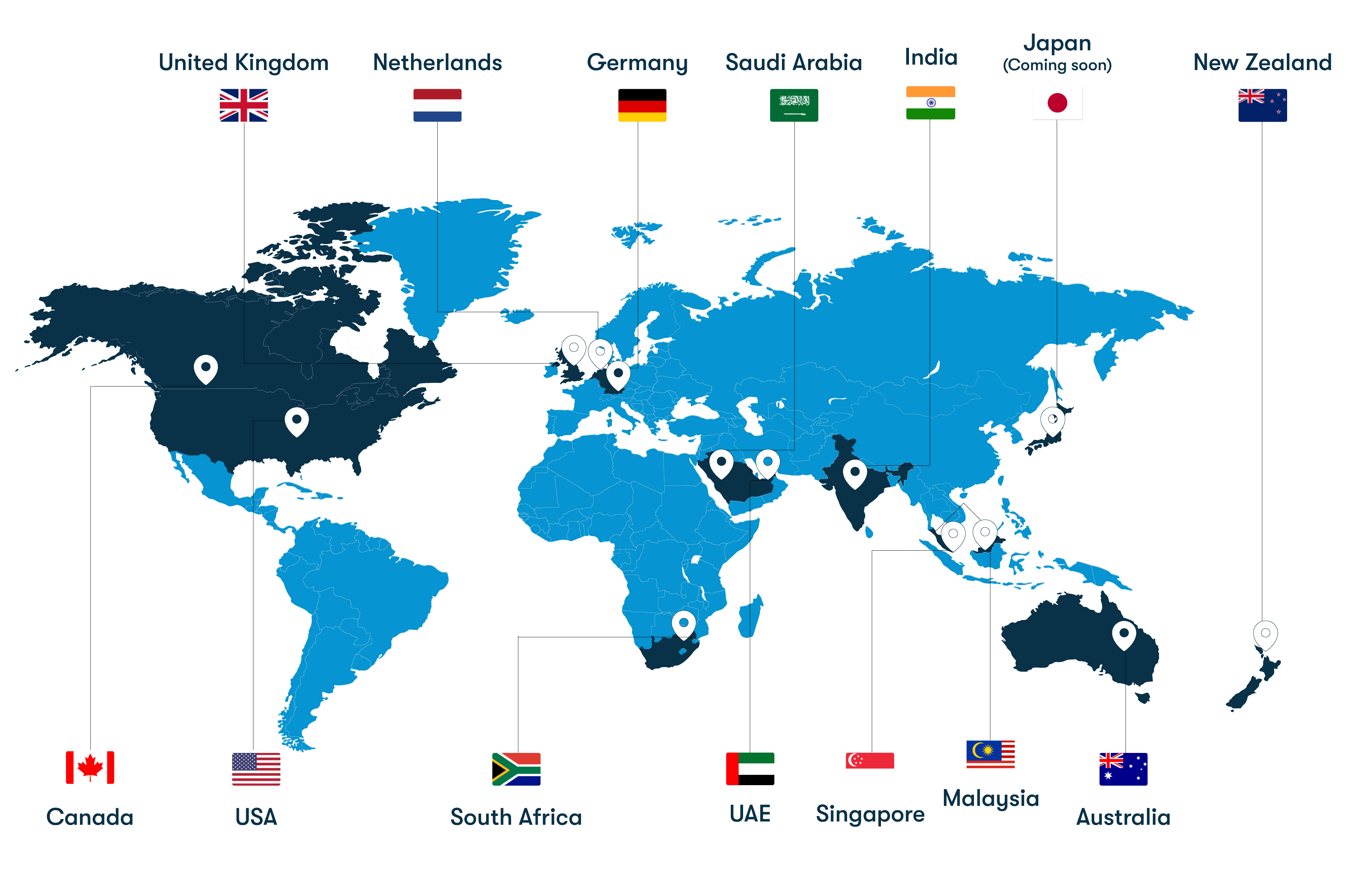
From our headquarters in India to training centers across UAE, Iraq, Saudi Arabia, UK, USA, Singapore, Australia, and more — Koenig delivers Microsoft certification training in 50+ countries.
50+
Countries
500K+
Trained
33+
Years
95%
Pass Rate
Koenig training locations worldwide